A design and simulation environment rooted in photonics, expanding towards optical, electronic and mechanical systems — from millimetres through micrometres to nanometres.
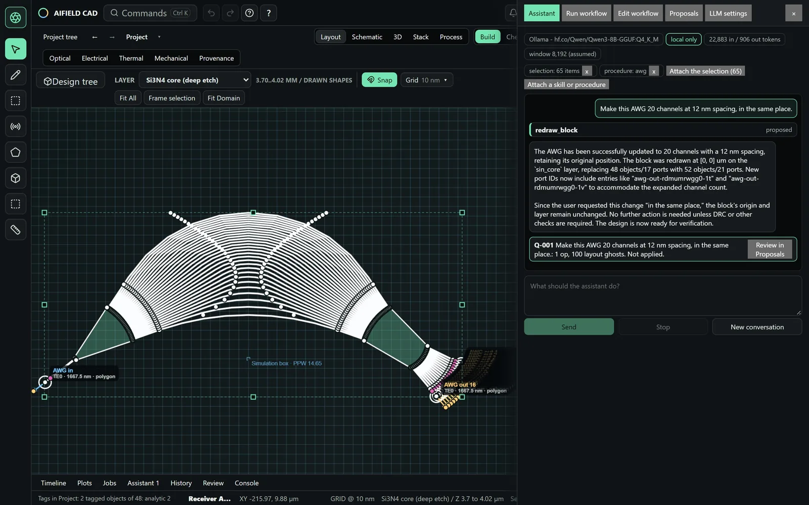
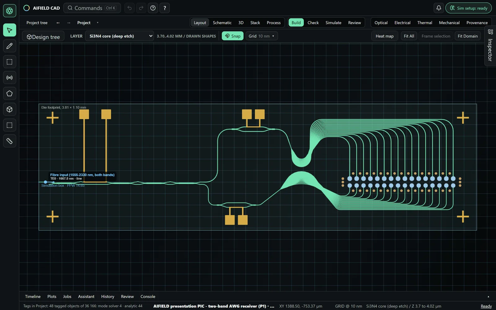
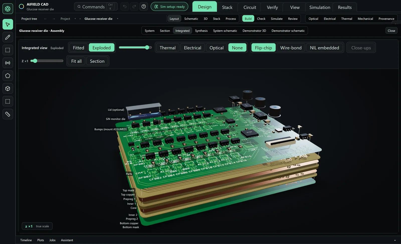
Screenshots of AIFIELD as it runs today: the AI assistant proposing a change, a receiver test chip, and the chip on its readout board.
The assistant proposes, the designer decides. A request to widen an AWG to 20 channels, drawn on the layout as ghosts and waiting for approval.Screenshot · AIFIELD CAD · 7 Oct 2026A receiver test chip around two AWGs. 32 spectral channels, 15 nm apart, in two bands. Designed, not yet fabricated.Screenshot · AIFIELD CAD · 12 Oct 2026The chip and its readout board, designed together. An exploded assembly view; the packaging details are assumptions.Screenshot · AIFIELD CAD
AIFIELD / ONE DESIGN, CONNECTED PHYSICS
A voltage. A movement. A new path for light.
Follow an electrical input through a moving microstructure, optical routing and electronic readout. Touch the driver to begin.
Explore the connections
One input, four connected responses.
Drag the driver left or right. The applied voltage moves the suspended guide, changes the optical split and updates both detector outputs.
Drive4.00 VMovement— nmOptical gap— nmOutput A / B— / —
Driver: voltage · source: wavelength and amplitude · empty space: rotate. Keyboard arrows work too.
Geometry, equations & assumptions
Public conceptual layout, not the ArtiSense product. The drawing shows a subset of fingers and an insulated buried feed beneath the moving frame. An in-plane electrostatic comb drive is coupled to a linear spring and an ideal lossless directional coupler. F = Nε₀tV²/g; x = F/k, limited by a 450 nm mechanical stop. Assumed: 80 finger pairs, 220 nm thickness, 1.2 µm electrode gap, k = 0.012 N/m; optical gap 650 → 200 nm. Optical coupling uses an assumed exponential gap dependence and a 24 µm interaction length. Input power = field amplitude² × 1 mW. Detector responsivity 0.55 A/W and TIA gain 1 kΩ are constant assumptions; 5% of output B feeds the grating detail. No losses, noise, dynamic mechanical solve, stress field, temperature or fabrication qualification are claimed. This is an analytical compact model, not a FEM/FDTD result. NIR light uses false colour.
06 / OBSERVE THE OUTPUT
From the guide into free space.
The 5% monitor tap from output B feeds this grating detail. Its source wavelength follows the module above; change either input to explore the same state.
Light leaving the chip
Change the wavelength at the input. Inspect the angular intensity on a projected observation plane.
Touch the input dot to steer the beam. Drag empty space to rotate.
Geometry & model
20 native curved teeth, 320 nm core. A lightweight uniform-array approximation uses the mean grating index and period of the 850 nm design: sin θ = n_eff − λ/Λ. The observation plane shows normalised angular array-factor intensity, with an assumed Gaussian transverse envelope. Its position is schematic, not a propagation-distance measurement. No solved 3D field or coupling efficiency is claimed. The native chirp, polarization, material dispersion and substrate radiation are not solved here. Near-infrared wavelengths 750–950 nm use false colour; the visible AWG is a separate design.
The project
From a design question to an inspectable result.
Photonics is AIFIELD’s starting point. Our goal is one environment for micro-optics, photonic circuits, micro- and nanoelectronics, MEMS and mechanical design, across millimetre, micrometre and nanometre scales. Today the photonic workflow is the most mature: geometry, layers and processes, with optical, circuit and thermal modelling. The other domains are earlier.
For engineers and researchers connecting optics, electronics and mechanics. We start from the photonic workflows we can already show and agree the scope each design needs.
Where the work stands
A clear view of the current work.
Updated October 2026
01 / DONE SO FAR
What we have done
We have built a photonic CAD with optical, circuit and thermal calculations, compared its engines against our own reference solver, designed a receiver test chip in it, and added an AI assistant whose proposals the designer reviews.
02 / STILL OPEN
What we still have to prove
Our comparisons are internal: they are not measurements on fabricated chips. Neural field prediction is still research, and we state its boundary conditions with every result.
03 / NEXT STEP
What comes next
Next: a reproducible demonstration, a clear account of what each tool can and cannot do, and the comparison conditions published with every result. Demos are arranged on request.